
SEMICONDUCTOR
WHAT IS A SEMICONDUCTOR?
A semiconductor device is an electronic component that uses electrical conduction but has traits that are in between that of a conductor, for instance copper, and that of an insulator, such as glass. These devices use electrical conduction in the solid state as opposed to in the gaseous state or thermionic emission in a vacuum, and they have replaced vacuum tubes in most modern applications.
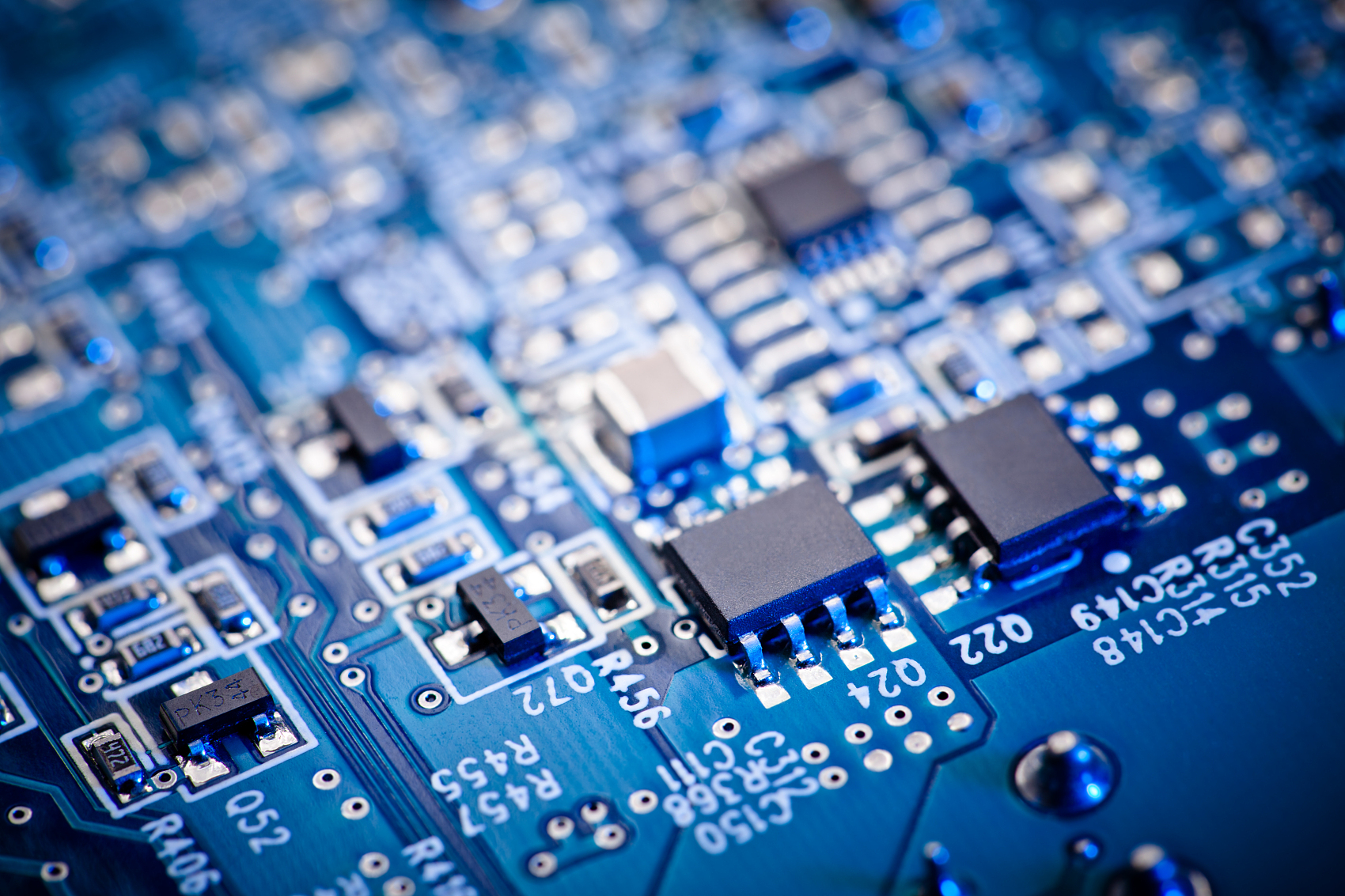
The most common use of semiconductors is in integrated circuit chips. Our modern computing devices, including mobile phones and tablets, might contain billions of tiny semiconductors joined on single chips all interconnected on a single semiconductor wafer.
The conductivity of a semiconductor can be manipulated in several ways, such as by introducing an electric or magnetic field, by exposing it to light or heat, or due to the mechanical deformation of a doped monocrystalline silicon grid. While the technical explanation is quite detailed, the manipulation of semiconductors is what has made our current digital revolution possible.

HOW IS ALUMINUM USED IN SEMICONDUCTORS?
Aluminum has many properties that make it a primary choice for use in semiconductors and microchips. For instance, aluminum has superior adhesion to silicon dioxide, a major component of semiconductors (this is where Silicon Valley got its name). It’s electrical properties, namely that it has low electrical resistance and makes for excellent contacting with wire bonds, are another benefit of aluminum. Also important is that it’s easy to structure aluminum in dry etch processes, a crucial step in making semiconductors. While other metals, like copper and silver, offer better corrosion resistance and electrical toughness, they are also much more expensive than aluminum.
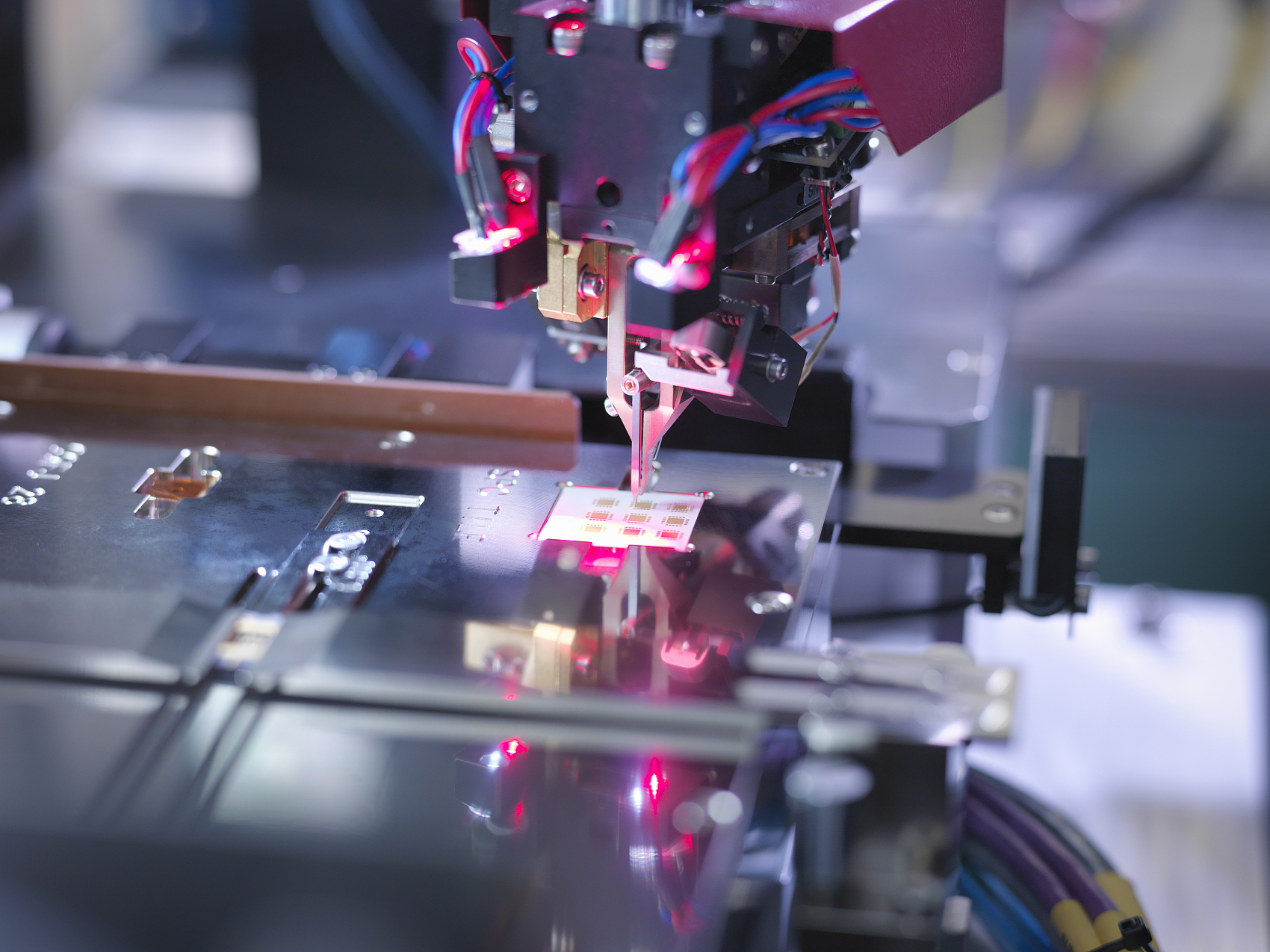
One of the most prevalent applications for aluminum in the manufacture of semiconductors is in the process of sputtering technology. The thin layering of nano thicknesses of high-purity metals and silicon in microprocessor wafers is accomplished through a process of physical vapor deposition known as sputtering. Material is ejected from a target and deposited on a substrate layer of silicon in a vacuum chamber that has been filled with gas to help facilitate the procedure; usually an inert gas such as argon.
The backing plates for these targets are made of aluminum with the high purity materials for deposition, such as tantalum, copper, titanium, tungsten or 99.9999% pure aluminum, bonded to their surface. Photoelectric or chemical etching of the substrate’s conductive surface creates the microscopic circuitry patterns used in the semiconductor’s function.
The most common aluminum alloy in semiconductor processing is 6061. To ensure the best performance of the alloy, generally a protective anodized layer will be applied to the surface of the metal, which will boost the corrosion resistance.
Because they are such precise devices, corrosion and other problems must be monitored closely. Several factors have been found to contribute to corrosion in semiconductor devices, for instance packaging them in plastic.